PROCESSOR DEVELOPMENT FROM GENERATION TO GENERATION
PCs are designed based on different CPU generations. Intel is not the only company that makes CPUs, though that pioneers among others. In each generation that dominates are Intel chips, but in the fifth generation there are several options other than Intel chips.
The processor is a very important part of a computer, which functions as the brain of a computer. No computer processor is just a dumb machine that can not do anything. Processors that we use today is very fast. Of course to achieve speed until now the processor is progressing. Well following the development of processors ranging from 4004 microprocessor generation in use on the busicom counter to the Quad-core Xeon intel.
The development of the processor was preceded by an intel processor at that time only one of its microprocessors existed. But at this time has many outstanding processors from other manufacturers, so that users can get a variety of processors.
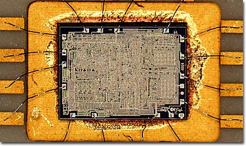
1. Microprocessor 4004 (1971)
2. Microprocessor 8008 (1972)
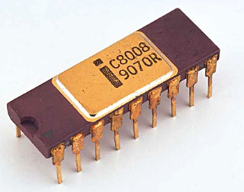
In 1972 intel issued a microprocessor 8008 speed of 2-fold count of the previous MP. This MP is the first 8 bit mp. Mp is also designed to do one job only.
3. Microprocessor 8080 (1974)
3. Microprocessor 8080 (1974)
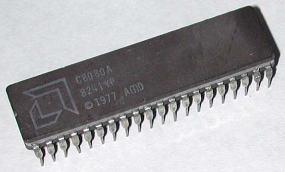
This year also comes mp from other manufacturers such as the MC6800 from Motorola -1974, Z80 from Zilog -1976 (two rivals heavy), and other Mega 6500 series processors, Rockwell, Hyundai, WDC, NCR and so on.
GENERATION 1 (Processor 8088 and 8086)
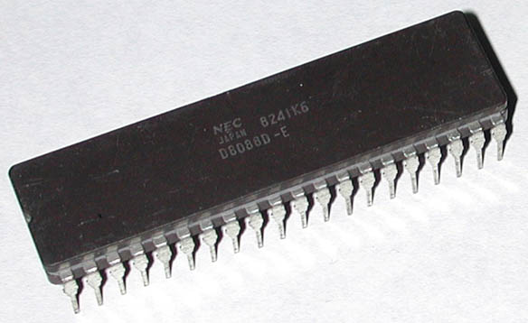
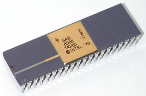
Actually 8088 is a 16/8 bit CPU. Logically this processor can be named 8086SX. 8086 is the first CPU that really 16 bits in this family.
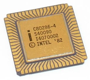
GENERATION 2 Processor 80286
GENERATION 3 Processor 80386 DX
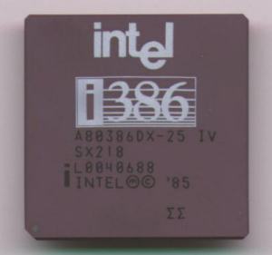
386 launched October 17, 1985. 80386 is the first 32 bit CPU. From a traditional PC DOS point of view, not a revolution. The good 286 works as fast as the first 386SX-despite applying 32 bit mode. This processor can address up to 4 GB of memory and has a better way of addressing than 286. 386 works at clock speeds of 16.20, and 33 MHz. Later Cyrix and AMD made clones that worked at 40 MHz. 386 introduces a new working mode in addition to real and protected mode in 286. The new mode is called virtual 8086 that opens for multitasking because the CPU can create multiple virtual 8086s in each of its own memory locations. 80386 is the first CPU to work well with early versions of Windows.
Processor 80386SX
This chip is a complete incomplete chip from 386DX. This processor has only a 16 bit external data bus different from the 32 bit DX. Also, SX only has 24 address lines. Therefore, this processor can only address a maximum of 16 MB of RAM. This processor is not the real 386, but the cheaper motherboard makes it very popular.
GENERATION 4 Processor 80486 DX
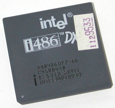
80486 issued April 10, 1989 and works twice as fast than its predecessor. This can happen because handling x86 commands is faster, especially in RISC mode. At the same time the bus speed is raised, but 386DX and 486DX are 32 bit chips. Something new in 486 is to make one math coprocessor / mathematical auxiliary processor.
Previously, the math co-processor that had to be installed was a separate 387 chip, 486 also had an 8 KB L1 cache.
Processor 80486 SX
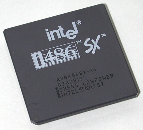
This processor is an incomplete new chip. Math co-processor removed compared to 486DX. Processor Cyrix 486SLC
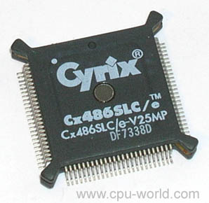 Cyrix and Texas Instruments have created a series of 486SLC chips. The chips use the same set of commands as 486DX, and work internally 32 bit like DX. But externally it works only on 16 bits (like 386SX). Therefore, the chips only handle 16 MB of RAM. Moreover, it has only 1 KB internal cache and no mathematical co-processor. Actually the chips are only a 286 / 386SX improvement. The chips are not clone chips. The chips have a fundamental difference in architecture compared to Intel chips.
IBM 486SLC2 Processor
IBM has a homemade 486 chip. The series of chips are named SLC2 and SLC3. The latter is known as Blue Lightning. These chips can be compared with Intel's 486SX, because they do not have a single mathematical coprocessor. But it has an internal cache of 16 KB (compare with Intel which has 8 KB). What reduces performance is the bus interface of the 386 chip. SLC2 works on 25/50 MHz externally and internally, while the SLC3 chip works on 25/75 and 33/100 MHz. IBM makes these chips for their own PCs with their own facilities, logically logging them from Intel.
Further developments
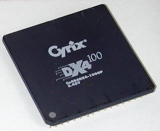
DX4; The Intel DX4 processors represent an increase of 80486. The speed is threefold from 25 to 75 MHz and from 33 to 100 MHz. Other DX4 chips are accelerated from 25 to 83 MHz. DX4 has an internal cache of 16 KB and works on 3.3 volts. DX and DX2 only have 8 KB cache and require 5 volts with built-in hot problems.
GENERATION 5 Pentium Classic (P54C)
This chip was developed by Intel and released on March 22, 1993. Pentium processor is super scalar, which means this processor can run more than one command per tick clock. This processor handles two commands per tick, comparable to two 486 in one chip. There is a major change in the system bus: its width is doubled to 64 bits and its speed increases to 60 or 66 MHz. Since then, Intel has produced two Pentiums working on the 60 MHz bus system (P90, P120, P150, and P180) and the rest, working on 66 MHz (P100, P133, P166, and P200).
Cyrix 6 × 86
The chip from the Cyrix company introduced February 5, 1996 is an inexpensive Pentium clone. This chip is compatible with Pentium, as it fits with Socket 7. Cyrix markets its CPUs by comparing at Intel clock frequency. Cyrix 6 × 86 is known for poor performance on its floating point. Cyrix has problems running NT 4.0.
AMD (Advanced Micro Devices)
Pentium-pentium AMD as chips offered by Intel compete tightly. AMD uses their own technologies. Therefore, the processor is not a clone-clone. AMD has the following series: - K5, can be likened to Pentium-pentium Classic (with 16 KB L1 cache and without MMX).
- K6, K6-2, and K6-3 compete with Pentium MMX and Pentium II.
- K7 Athlon, August 1999, not compatible with Socket 7.
AMD K5
K5 is a Pentium imitation. The old K5 as an example is sold as PR133 (Perform Rating). That is, that the chip will work like a Pentium P133. However, it only runs 100 MHz internally. The chip still has to be mounted on the motherboard like a P133. K5 AMD also have the PR166. This chip is meant to compete with the Intel P166. Works only at 116.6 MHz (1.75 x 66 MHz) internally. This is because the cache is optimized and other new developments. There are only features that do not comply with P166 that is in floating-point work. PR133 and PR166 are worth much cheaper than the comparable Pentium type, and this processor is very popular on machines with low prices.
Pentium MMX (P55C)
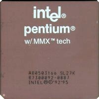
Pentium-pentium P55C was introduced January 8, 1997. MMX is a collection of new commands (57 new integers, 4 new data types and 8 64-bit registers), which adds to the CPU's capabilities. MMX commands are designed for multimedia programs. Programmers can use this command in their programs. This will provide improvements in running the program.
Winchip IDT
IDT is a smaller company that generates CPUs such as Pentium MMX at low prices. The first WinChip C6 IDT was introduced in May 1997.
AMD K6
K6 AMD launched April 2, 1997. This chip works slightly better than Pentium MMX. It is therefore included in the P6 family.
· Comes with 32 + 32 KB L1 and MMX cache.
· Contains 8.8 million transistors.
K6 as well as K5 compatible with Pentium. Then, it can be placed in Socket 7, on most Pentium motherboards, and this soon makes K6 very popular.
Cyrix 6 × 86MX (MII)
Cyrix also has a chip with a high performance, is between the 5th and 6th generation. The first type was seated against the Pentium MMX chip from Intel. The next type can be compared with K6. The powerful P6 group processor from Cyrix was announced as "M2". Introduced on May 30, 1997 the name became 6 × 86MX. Then named MII. The 6 × 86MX chip is compatible with Pnetium MMX and paired on a regular Socket 7 motherboard, 6 × 86MX has 64 KB of internal L1 cache. Cyrix also leverages technology that is not found inside the Pentium MMX. 6X86MX is specifically compared to other 6th generation CPUs (Pentium II and Pro and K6) because it does not work based on the RISC kernel. 6X86MX runs the original CISC commands like Pentium MMX. 6X86MX has - like all Dary Cyrix processors - issues related to FPU units. However, if only used for standard applications, this is not a problem. Problems will arise if playing 3D games. 6 × 86MX chip is powerful enough. But these chips do not have FPU and MMX that work well. These chips do not incorporate 3DNow technology!
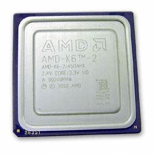
AMD K6-2The next version of "model 8" K6 has the code name "Chomper". The processor on 28 May 1998 is marketed as K6-2, and like the original 7 K6 model version, made with 0.25 micron technology. These chips work only with 2.2 volt. This chip managed to become a rival Intel Pentium II. K6-2 is made for front side bus (system bus) at 100 MHz speed and Super 7 motherboard. AMD makes other companies like Via and Alladin, making new chip sets for traditional Socket 7 motherboards, after Intel knows 1997 to stop the platform. K6-2 is also improved with MMX performance which is twice as good as the initial K6. K6-2 has a new 3D plug-in (called 3DNow!) For better gaming performance. It consists of 21 new commands that can be used by software developers to provide better 3D performance.
Support is included in DirectX 6.0 for Windows. DirectX is a multimedia API, for Windows. DirectX is some program that can improve multimedia performance in all Windows programs. 3DNow Multimedia! not compatible with MMX, but K6-2 has MMX as well as 3DNow !. Cyrix and IDT also launch the CPU with 3DNow !.
K6-2 gives very, very good performance. You can compare this processor with Pentium II. K6-2 350 MHz work very similar to Pentium II-350, but sold cheaper. And can save more because the motherboard is cheaper.
GENERATION 6 Pentium Pro
The development of Pentium Pro began in 1991, in Oregon. Introduced on November 1, 1995. Pentium Pro is a pure RISC processor, optimized for 32 bit processing on Windows NT or OS / 2. The new feature is that the L2 cache is a single giant chip, with a rectangular chip and Socket-8. CPU and L2 cache units are separate units inside this chip.
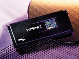
Pentium II
Pentium Pro "Klamath" is the code name of Intel's top processor. This processor terminates the Pentium Pro series, which is partly reduced and in part there are improvements.
Introduced May 7, 1997, the Pentium II features:
· CPU is put together with 512 KB L2 in a SECC module (Single Edge Contact Cartridge)
· Connects with the motherboard using a slot one and a GT6 + P6 bus.
· MMX commands.
· Fixed running 16 bit program (nice for Windows 3.11 users)
· L1 cache replication and repair (16 KB + 16 KB).
· Internal speed increases from 233 MHz to 300 MHz (next version is higher).
· L2 cache works at half the CPU speed.
With the new design, L2 cache has its own bus. The L2 cache works at half the CPU speed, such as 133 MHz or 150 MHz. It is definitely a throwback from Pentium Pro, which can work on 200 MHz between CPU and L2 cache. This is answered with L1 cache. Below is the comparison:
Pentium II has been available in 233, 266, 300, 333,350, 400, 450, and 500 MHz (higher speeds soon emerge). With chip set 8244BX and i810 Pentium II has a very good performance.
Pentium II is a large rectangular plastic box, containing CPU and cache. There is also a small controller (S824459AB) and a large size cooling fan.
Early 1998 Intel had a difficult time with a rather expensive Pentium Pro II. Many users buy AMD K6-233M, which offers excellent performance at a decent price.
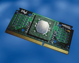
So Intel makes a brand new CPU called Celeron. This processor is the same as Pnetium II except the removable L2 cache. This processor can be called the Pentium II-SX. In 1998 Intel replaced its Pentium MMX with the first Celeron. Then the design is improved. The Celeron cartridge complies with Slot 1 and works on a 66 MHz bus system. The internal clock works on 266 or 300 MHz.
Pentium-II Celeron A: Mendocino
 technoportmedia.blogspot.com
An interesting part of the new cartridge with 128 KB of L2 cache inside the CPU. This gives a very good performance, because the L2 cache works at full CPU speed. Celeron 300A is a chip in the card:
Pentium-II Celeron PPGA: Socket 370
http://www.tradenote.net/
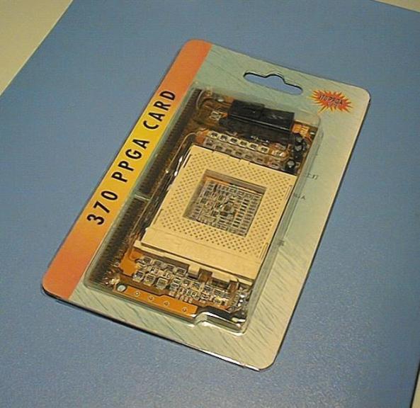
New Socket 370 for Celeron. Processors 400 and 366 MHz (1999) are available in a plastic pin grid array (PPGA). The PGA370 socket looks like a traditional Socket 7 that has 370 pins.
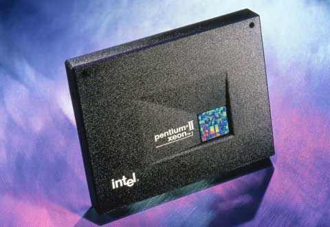
Pentium-II Xeon
 http://www.prof2000.pt
On 26 January 1998 Intel introduced a new Pentium II cartridge named Xeon. Intended for high-end servers and users. Xeon is a new Pentium II cartridge dash corresponding to a new connector called Slot two. This module is two cal higher than Pentium II, but there are other important changes and improvements:
· New RAM L2 cache type chip: CSRAM (Custom SRAM), which works at full CPU speed.
· Different L2 cache size: 512, 1024, or 2048 KB RAM L2.
· Up to 8 GB of RAM memory can be cached.
· Up to four or eight Xeons in one server.
· Supports clustered servers.
· New chip set 82440GX and 82450NX.
Xeon chips work at full CPU clock speeds. Can be expected, that will have the same performance as L1 cache. But the interface from L1 to L2 is worth a few ticks tick at the beginning of each switch, so there is some slowness. But if the data has been moved, it works at full clock speed.
AMD K6-3
(http://www.m571.com)
AMD K6-3 is a model 9 codenamed "Sharptooth", which may have a three-level cache:
· Few improvements compared to units K6-2
· L2 cache of 258 KB one chip
· A three level cache design
· New 133 MHz front side bus.
· 400 MHz clock speed with 450 MHz.
Both 64 KB L1 and 256 KB L2 cache are combined with the chip. The Cache on die L2 works at full processor speeds as performed on Pentium Pro, and as performed on Celeron A and on Intel Xeon processors.
This will definitely increase K6 speed a lot! Because K6-3 is used on Super 7 motherboards and space for cache the next level of L3 cache. The design of a three-level cache is made to use an existing motherboard up to 2 MB of on-board cache. This should be the L2 cache (on the motherboard) used as the third level cache. This happens automatically, and the bigger the cache name will increase its performance a lot!
Pentium III - Katmai
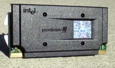
The first P6 CPU from Intel is the Pentium Pro. Then we got the PentiumII in various types. And the last is Pentium III. March 1999 Intel introduced the newly enhanced MMX2 collection for graphical perintayh (70 of them). This command is called Katmai New Instructions (KNI) / New Order Katmai or SSE. This command is intended to improve the performance of 3D games - such as 3DNow technology! AMD. Katmai includes "double precision floating-point single instruction multiple data" / "floating point with multiple precision one data command" (or DPFS SIMD for brevity) that works in eight 128 bit registers.
KNI was introduced in the new 500 MHz Pentium III. This processor is very similar to Pentium II. Using Slot 1, and just different on new features like Katmai and SSE support.
This processor is mounted on the motherboard with BX chip set and slot 1.
This processor has several features:
· Number of identifiers
· New register and 70 new commands
Finally the clock speed is raised up to 500 MHz with room for further improvement. The Pentium III Xeon (codenamed Tanner) was introduced March 17, 1999. The Xeon chip is updated with all the new features of the Pentium III. To make use of it Intel has announced the Profusion chip set.
The PSN identifier number (Processor Serial Number), unique to each CPU, has led to many security issues. This number is worth 96 bits programmed electronically into each chiop. In fact this means a very wise initiative, which can make electronic commerce and encryption within the Internet safe and effective.
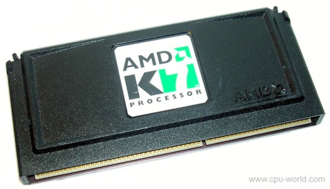 GENERATION 7 AMD K-7 Athlon
AMD's most staggering mainstream AMD processor was introduced in August 1999. Intel's response (Foster's code name) could not be expected until the end of 2000. In the first months, the market responded to Athlon very positively. It seems (as expected) to outperform the Pentium III at the same clock frequency.
· Like the modules on the Pentium II, which designs fully belong to AMD. The socket is called Slot A.
· 600 MHz clock speed is the first version.
· L2 cache reach 8 MB (minimum 512 KB, no additional TAG-RAM).
· 128 KB L1 cache.
· Contains 22 million transistors (Pentium III has 9.3 million).
· New bus type
· A completely new system bus type, which in the first version will work at 200 MHz. An increase of up to 400 MHz is expected later. 200MHz RAM speed is twice as fast as all existing Intel CPUs. This high speed will require new fast RAM to take full advantage of this effect.
· Free backside bus, connecting L2 cache. Here the clock speed can be ¼, 1/3, 2/3 or equal to the internal CPU frequency. It is the same system as used on P6 systems where the speed of L2 can be half (Celeron, Pentium II and III) or full CPU speed (like Xeon).
· Strong encoding and DPU
· Three command-coders translate the RISCx86 program command to an effective RISC command, ROP, where up to 9 commands can be executed serendively. The first test shows the encoding of 2.8 CISC commands per clock cycle. It is approximately 30% better than Pentium II and III.
· Can handle and rearrange up to 72 orders (outside ROP) simultaneously (Pentium III can do 40, K6-2 only 24).
· Great FPU performance with three simultaneous commands and one GFLOP on 500 floating point. Two GFLOP with MMX and 3DNow commands! It is at least the same as the Pentium III performance by fully utilizing Katmai. 3DNow Engine! even improved compared to K6-3.
· AMD has no license to use Slot 1 design, so the controller logic circuit comes from Digital Equipment Corp. Called EV6 and designed for Alpha 21264 CPU. AMD companies plan to develop their own chip set, but the design will be royalty free to use. This makes the first AMD processor that uses motherboards and chip sets designed specifically by AMD itself.
· The use of EV6 buses gives a lot more band width than Intel GTL +. This means that Athlon has the ability to work with new RAM types such as RDRAM. Also the use of 128 KB of L1 cache is quite heavy. The L1 cache is important if the clock speed is increased and 128 KB is twice the size of the Pentium II.
· Athlon will be present in several versions. The "slowest" version has L2 cache that works one-third of the CPU speed, which works best at full CPU speed (as Xeon does). Athlon will provide Intel's competitions in all levels including servers, which can be compared with Xeon processors.
8th Generation Intel Core 2 duo
8th generation processor is Core 2 Duo which was launched in July 2007. This processor uses microprocessor with x86 architecture. The architecture by Intel is called Intel Core Microarchitecture, where the architecture replaces the old architecture from Intel called NetBurst since 2000 ago. The use of Core 2 also marks the era of the new Intel processor, where the Intel Pentium brand that has been in use since 1993 was replaced with Intel Core.
At this time Core 2 design is very different from NetBurst. On NetBurst that is applied in Pentium 4 and Pentium D, Intel put forward a very high clock speed. While on the new Core 2 architecture, Intel is more emphasis on the increase of the features of the CPU, such as cache size and the number of cores that exist in Core 2 processor. Intel party claims, the power consumption of the new architecture requires only very little power compared to the previous Pentium processor lineup.
Intel Core 2 processor has features such as EM64T, Virtualization Technology, Execute Disable Bit, and SSE4. Meanwhile, the latest technology is carried LaGrande Technology, Enhanced SpeedStep Technology, and Intel Active Management Technology (iAMT2).
Here are some codenamed of processor cores found on Intel Core 2 processor products, of course the codenamed have differences between each other.
CONROE
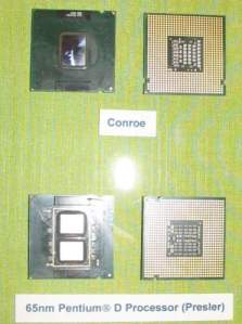
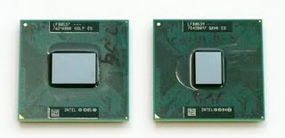
Core processors from Intel Core 2 Duo are first codenamed Conroe. The processor is built using 65 nm technology and is intended for desktop use to replace the Pentium 4 and Pentium D line. Even the Intel claims that Conroe has a 40% better performance compared to Pentium D which must have been using dual core as well. The Core 2 Duo only requires 40% less power than the Pentium D to produce the above mentioned performance.
Processors that already use the Conroe cores are labeled with "E6 × 00". Several types of Conroe that have been circulating in the market is type E6300 with clock speed of 1.86 GHz, type E6400 with clock speed of 2.13 GHz, type E6600 with clock speed of 2.4 GHz, and type E6700 with clock speed of 2.67 GHz. For processors with type E6300 and E6400 have Shared L2 Cache of 2 MB, while the other type has L2 cache of 4 MB. The lineup of this processor has a FSB (Front Side BUS) of 1066 MT / s (Megatransfer) and the power required is only 65 Watt TDP (Thermal Design Power).
Based on the testing that is in some sites that we found, up to this writing down the processor from the Core 2 family is able to rival the enemy magnitude, namely AMD. And when overclocking up to 4 GHz though, processor with type E6600 and E6700 still able to work in stable even though multipliers owned very limited. The results break the notion of an overclocking community who think that Intel's processors are not to be overclocked. In fact, some of the processors tested by some of these sites, Intel Core 2 Duo even able to outperform AMD which has been a long time "king" of the line of processors used for desktop especially 3D Now!
 CONROE XE
The next Core processor is Conroe XE which is currently a lot of talks. Conroe XE itself is a core processor from Intel Core 2 Extreme which was launched simultaneously with Intel Core 2 Duo on July 27, 2006. Conroe XE has more power compared with Conroe. The first and the only type released by Intel for the Core 2 Extreme processor line is the X6800 and is already on the market today despite the very limited number.
Intel Core 2 processor that is already using Intel Core 2 Extreme with core Conroe XE will replace the position of the Pentium 4 EE (Extreme Edition) and Dual Core Extreme Edition. Core 2 Extreme has a clock speed of 2.93 GHz and a FSB of 1066 MT / s. The family of Conroe XE requires a TDP of only 75 to 80 Watts. In the state of full load temperature processor of X6800 produced will not exceed 450C. Another if the SpeedStep function is in the active state. If active, then the processor temperature when idle state produced by X6800 only about 250C. Quite impressive, considering the previous generation Intel Pentium 4 Extreme Edition processor produces heat that can be said to be very high.
Almost the same as Core 2 Duo, Core 2 Extreme has a shared L2 cache of 4 MB only the most visible difference from both Conroe is the speed of each clock speed alone. Actually for an "Extreme Edition" class of processors, the difference should be even more, not just based on the size of its clock speed alone. In addition to the difference in clock speed, Core 2 Extreme features to change multipliers up to 11x (step) to get maximum overclocking results. Other unique features included in Core 2 Extreme Edition this time are larger FSB, L2 cache larger, and the existence of L3 cache.
Intel Core 2 Extreme Edition with X6800 type has 36% higher performance compared to AMD Athlon 64 FX-62. Core 2 Extreme Edition X6800 can be overclocked to 3.4 GHz just by using a standard heatsink only, the ability is quite extraordinary we think because then you do not need additional funds for a heatsink.
 AMD Athlon 64
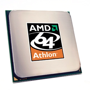
Released on September 23, 2003, the Athlon 64 is AMD's first production processor for the K8 CPU family intended for the desktop and laptop computer market. Simultaneously, AMD also released the Athlon 64 FX, another version of the Athlon 64 intended for enthusiast users.
The main feature of the K8 architecture is the implementation of 64-bit technology (AMD64). Although it operates as a 64-bit processor, Athlon still supports 8-bit, 16-bit, and 32-bit applications. In addition, there are some basic features that K8 architecture has, such as:
L1-cache of 128KB, while the capacity of L2-cache varies, among others 512KB or 1MB, depending on the variant.
The memory controller is integrated on the processor so it runs with the same clockrate as the clockrate processor. Data access to memory is also "short" compared to when the memory is in "north bridge" so that it can reduce the latency significantly.
Using Hyper Transport (HT) technology to convert traditional FSB where processor is connected with other components by using links with higher bandwidth, and lower latency.
Support for SSE2 instructions and from Arhlon 64 revision cores E3 (Venice), added support for SSE3 instructions.
Athlon 64 initially used a 130 nm manufacturing process, then switched using a 90 nm, and 60 nm manufacturing process. Support processor used Athlon 64, namely:
"Socket 754", uses 64-bit memory interface (Single Channel), and Hyper Transport 800 MHz frequency.
"Socket 939", uses 128-bit memory interface (Dual Channel), and 1000 MHz Hyper Transport frequency.
"Socket AM2", which for the first time supports the use of DDR2 SDRAN memory to increase memory bandwidth up to 12.8 Gb / sec.
As for Athlon 64 FX, in addition to using "Socket 939" and "Socket AM2", also uses "Socket 940" and "Socket F".
The first processor that uses the K8 architecture is AMD Opteron. This processor was released on April 22, 2003, and is a Server / workstation class processor. AMD Opteron is manufactured with a choice of frequencies 1400 MHz - 3000 MHz, using "Socket 939" and "Socket 940". AMD Opteron is designed in 3 versions, namely: Processor for system uni-processor, dual-processor system, and system with 4 to 8 processor.
Pentium 4 Prescott
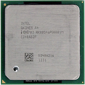 Although using the name Pentium 4, processor that was released February 1, 2004, the architecture has undergone a change from the previous Pentium 4 architecture. The processor is manufactured to meet Intel's ambition of reaching the pipeline processor, and becoming one of the power-hungry processors.
Pentium 4 Prescott is redesigned in two versions, supporting Hyper-Threading technology with FSB 800 MT / s, and which does not support Hyper-Threading technology with FSB 533 MT / s. In addition to support for basic features such as "MMX", "SSE" and "SSE2" on all Prescott models, Intel also added the "SSE3" feature and L2-cache capacity to 1024 KB. For some models equipped with 64-bit technology support Intel 64 "(x86-64 implementation), and support for" XD bit "technology (NX bit implementation).
9th GENERATION
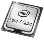
Intel Core 2
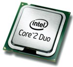
The Microprocessor Core 2 family was first introduced on July 27, 2006, based on the Intel Core microarchitecture. Produced in several versions, "Solo" (single-core / single into, available only in mobile version), "Duo" (dual-core / core), Quad (quad-core) 2007, "Extreme" version (Two or four core). Processor Core 2 Duo has two cores in sati die. While on the Core 2 Quad processor, Intel uses Multi-Chip Module technology, where the processor consists of two dies, and each die there with a Core 2 Duo.
In the Core 2 processor embedded 167 million to 820 million ransistor, using 65 nm and 45 nm technology. The capacity of L1-cache Core 2 is 64 KB on each core processor, while the L2-cache capacity varies between 2 MB, up to 12 MB (2 x 6 MB) and FSB between 533 MT / s up to 1600 MT / s, depending on model .
All Core 2 processor models support "MMX", "SSE", "SSE2", "SSE3", "SSSE3", "Enhanced Intel SpeedStep Technology" (EIST), "Intel 64" (x86-64) "XD bit "(Implementation of NX bit), as well as" iAMT2 "(Intel Active Management). For some models, Intel adds support for "Intel VT-x" features (Intel Virtualization Technologies for x86), "TXT" (Trusted Execution Technology), and "SSE4" (Penryn).
Although the Core 2 processor runs at a lower frequency compared to the Pentium 4, but with its more efficient architecture make the performance of Core 2 is much better.
The 9th Generation Transition
Intel Pentium D was released on May 25, 2005, a two-core processor whose two cores are not in one die. This processor has two dies each containing one core. This processor is based on Intel NetBurst micro-architecture and has almost all features of Prescott / Cedar Mill, plus some new features like "EIST", "Intel 64", "XD bit", as well as for some models also feature "Intel VT-x) . Overall, the Pentium D Performance Improvement is not very significant compared to Pentium 4, although it consumes higher power than the Pentium 4.
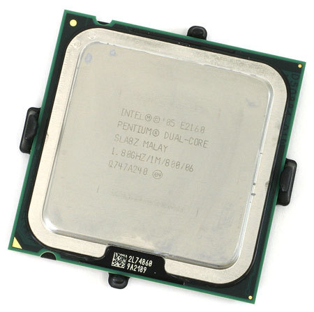 Intel Pentium Dual-Core
Although using the Pentium name, this processor is based on micro-architecture "Intel Core", so it has the basic features of microarchitecture "Intel Core". The new "Intel VT-x" feature support is available in the "Wolfdale-2M" series, and that is only for some models. Available clockspeed options are between 1.3 GHz to 2.8 Ghz with FSB 533 MHz, up to 1066 MHz, as well as 1MB-2MB L2-cache capacity.
maybe just a discussion about the history of the processor thanks.
